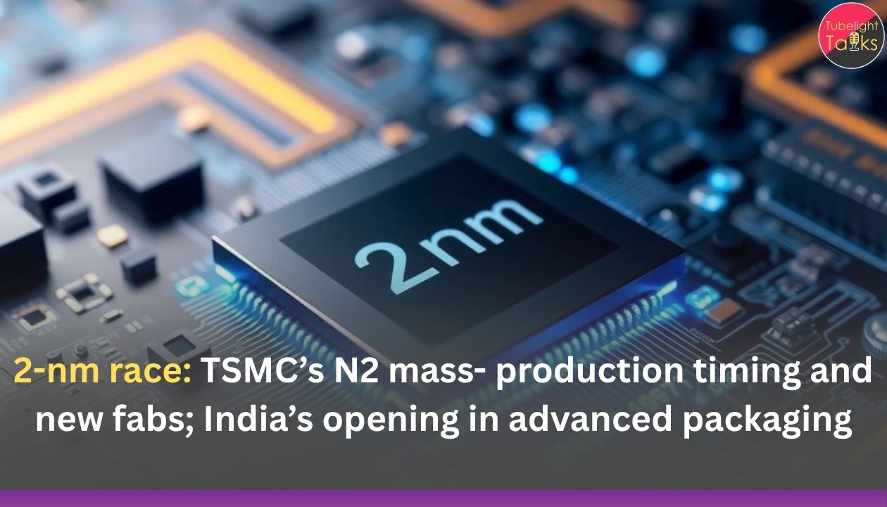
2-nm race: TSMC’s N2 mass- production timing and new fabs; India’s opening in advanced packaging
2-nm race: The most closely watched node in foundryland—TSMC’s 2-nm (N2)—is crossing from slides to silicon. Public briefings this year reiterated H2-2025 for N2 mass production and H2-2026 for the N2P shrink, with Fab 22 flagged as the 2-nm anchor and a third Arizona site planned for N2/A16 “by the end of the decade.”
In parallel, advanced packaging (CoWoS®, SoIC®) is surging to meet AI/HPC demand. India doesn’t print 2-nm wafers yet—but OSAT/ATMP projects (Tata, Micron) and a policy push create a credible on-ramp into advanced packaging, substrates, and test. Here’s the status, the sites, and a concrete India playbook.
What’s new on N2 (and what’s next)
- Mass-production window: TSMC reiterated N2 enters H2-2025, with N2P following in H2-2026. Independent symposium/analyst summaries and trade coverage have tracked the same dates.
- Fab anchor: TSMC’s own technology page notes “TSMC’s Fab 22 will be the 2-nm production facility.”
- Yield/defect signals: At 2025 tech events, TSMC said N2 (first GAA nanosheet) shows lower defect density than N3 at the same stage, with mass production targeted late Q4-2025—a useful proxy for ramp risk.
- Family roadmap: N2P is positioned as the performance/power uplift in 2H-2026; beyond that, A16 (1.6-nm-class) enters the conversation later in the decade.
Where the fabs are (quick map)
- Taiwan (Hsinchu/Kaohsiung): N2’s first waves are tied to Fab 22 and the Hsinchu/Kaohsiung cluster’s GIGAFABs.
- United States (Arizona): TSMC confirms Fab 1 (N4) in production, Fab 2 (N3) for 2028, and Fab 3 earmarked for N2/A16 with volume “by end of decade.”
- Europe (Dresden/ESMC): A JV fab for 28/22 and 16/12 nm (not 2-nm) expands footprint and auto supply; production by 2027.
- Japan (Kumamoto): Phase-1 (JASM) is live on mature nodes; Phase-2 timelines have faced press-reported delays (not 2-nm).
Why the 2-nm ramp is different (and packaging-led)
GAA nanosheets change device physics—but system performance now leans as much on packaging as on transistors. AI and chiplet designs need advanced packaging (CoWoS®, SoIC®, InFO) to stitch compute dies, SRAM, and HBM into one module. TSMC’s talks show CoWoS capacity CAGR >80% (’22–’26), and SoIC even faster, underscoring packaging as the true bottleneck. Expect N2-class wins to come packaged with 2.5D/3D advances, not as bare die.
Packaging capacity and customer demand: the state of play
- Capacity growth: TSMC’s symposium roadmaps highlight aggressive CoWoS/SoIC scale-up to meet HPC/AI orders.
- Utilization noise: Trade press has oscillated between “sold-out” and “under-utilized” narratives in 2025; the only safe conclusion is volatile, design-specific loading—another reason for buyers to dual-source packaging where possible.
India’s angle: from ATMP to advanced packaging (a credible near-term wedge)
What exists now
- Micron (Sanand) ATMP: India’s largest memory assembly & test project; strategic for building technicians, yield discipline, and supplier parks.
- Tata OSAT (Assam) + ecosystem build: A ₹27,000-crore OSAT complex is under way; Delhi-Mumbai & Northeast links are drawing equipment vendors (e.g., Tokyo Electron offices in Dholera and Assam), a sign of real supplier gravity.
- Policy signals: Government notes repeatedly stress packaging as a national lever to enter high-value silicon without waiting for leading-edge fabs.
What “advanced” can mean in 2026–27
- Fan-out & advanced 2.5D as the first rung (redistribution layers, large organic substrates, multi-die modules).
- HBM/AI substrate lines (ABF-class) co-located near OSATs to cut cycle time.
- Reliability labs (warpage, thermal cycling, high-speed SI/PI) to meet hyperscaler/auto qual.
India will not print N2 wafers in 2026, but it can package dies from TSMC/Samsung/Intel and capture value where cycle time and yield learning matter most.
What 2-nm + packaging means to buyers (chip firms and device OEMs)
- Total system perf/watt is now a node × package equation; HBM/IO topology and interposer size are as decisive as GAA perf.
- Slotting risk moves from wafer starts to packaging slots; secure two packaging paths (e.g., CoWoS-class + alternate fan-out) early.
- India as overflow: As Indian OSATs prove high-reliability lines, overflow/derivative SKUs can land there—shortening lead times for regional builds.
The 2026 watch-list (evidence-based checkpoints)
- N2 HVM: public confirmation of first N2 shipments and a follow-on N2P pilot in 2H-2026.
- Arizona Fab 3: site and tool milestones that keep an N2/A16 window “by decade’s end.”
- CoWoS/SoIC: quarterly disclosures on capacity adds and lead-time trends.
- India OSAT/ATMP: Tata (Assam) mechanical completion, first customer quals; Micron (Sanand) tool move-in → qual lots.
- Suppliers: ABF substrate & RDL/fan-out vendors announcing India footprints; test-handler and metrology service hubs nearby.
Principles for responsible scale
Great nodes don’t excuse bad habits. A simple ethic truthfulness, non-harm, service, restraint as guided by Enlightened Sant Rampal Ji Maharaj keeps the ramp human-centred: publish KPIs (safety incidents per million hours, energy/water per wafer-equivalent, RMA rate); use independent factory audits; and reserve affordable packaging/test slots for smaller design houses and university tape-outs so the upswing reaches the edges, not just the usual giants. These choices make advanced packaging a public good, not merely a margin centre.
Call to action
For Indian policymakers
Convert momentum into depth
- Tie OSAT incentives to CoWoS-adjacent capabilities (large organic substrates, RDL, SI/PI labs).
- Cluster equipment service hubs (etch, litho tracks, metrology) next to Assam/Gujarat sites.
- Co-fund substrate & underfill lines and talent academies (flip-chip, 2.5D warpage control).
For OSATs and EMS players
Land the first “advanced” lighthouse
- Start with fan-out + multi-die modules and HBM interposer assembly for data-centre boards.
- Publish third-party quals (temperature cycling, HTOL) to unlock hyperscaler/auto RFQs.
For design houses
Design for package early
- Treat package as a co-design domain; budget SI/PI and thermal from architecture stage.
- Book dual packaging routes (CoWoS-class + fan-out) to hedge slot volatility.
Read Also: India’s Chip Big-Bang: Dholera’s 28nm Fab, Jewar’s New Unit, Sanand’s OSAT
FAQs: 2-nm Race
1) When does TSMC’s 2-nm (N2) enter mass production?
TSMC guidance and symposium coverage point to H2-2025 for N2, with N2P following in H2-2026.
2) Which fab is the primary 2-nm site?
TSMC states “Fab 22 will be the 2-nm production facility.”
3) What’s the U.S. plan for 2-nm?
In Arizona, Fab 1 (N4) is in HVM, Fab 2 (N3) targets 2028, and Fab 3 is slated for N2/A16 volume by the end of the decade.
4) How fast is advanced packaging capacity growing?
TSMC’s talks cite >80% CAGR for CoWoS capacity through 2026, with SoIC rising even faster.
5) What is India’s realistic role near-term?
ATMP/OSAT: Micron (Sanand) and Tata (Assam) create a base to move into advanced packaging (fan-out, 2.5D, substrates), especially as equipment vendors open India offices.
6) Will Europe/Japan provide 2-nm capacity?
TSMC’s Dresden (ESMC) and Kumamoto projects focus on mature/FinFET nodes for auto/industrial; 2-nm remains centred in Taiwan (and the U.S. later in the decade).
Related Stories


Discussion (0)