Technology for Good: The “Light on a Chip” Optical Racetrack Breakthrough
Light on a Chip: Tuesday, February 24, 2026 brought a rare kind of tech headline – one that feels both futuristic and practical. Researchers have demonstrated chip-scale “optical racetrack” microresonators that trap light and let it circulate longer with dramatically reduced loss.
The University of Colorado Boulder team achieved this by redesigning the racetrack’s bends using smooth “Euler curves,” a geometry borrowed from road and railway engineering to avoid sharp turns that force light to leak out. Their message is simple but powerful: better design can mean less energy.
If scaled, such ultra-low-loss photonics could support greener sensors, more efficient communications, and new high-precision optical systems.
What Is an “Optical Racetrack” and Why Is Everyone Talking About It?
A racetrack made of light, not asphalt
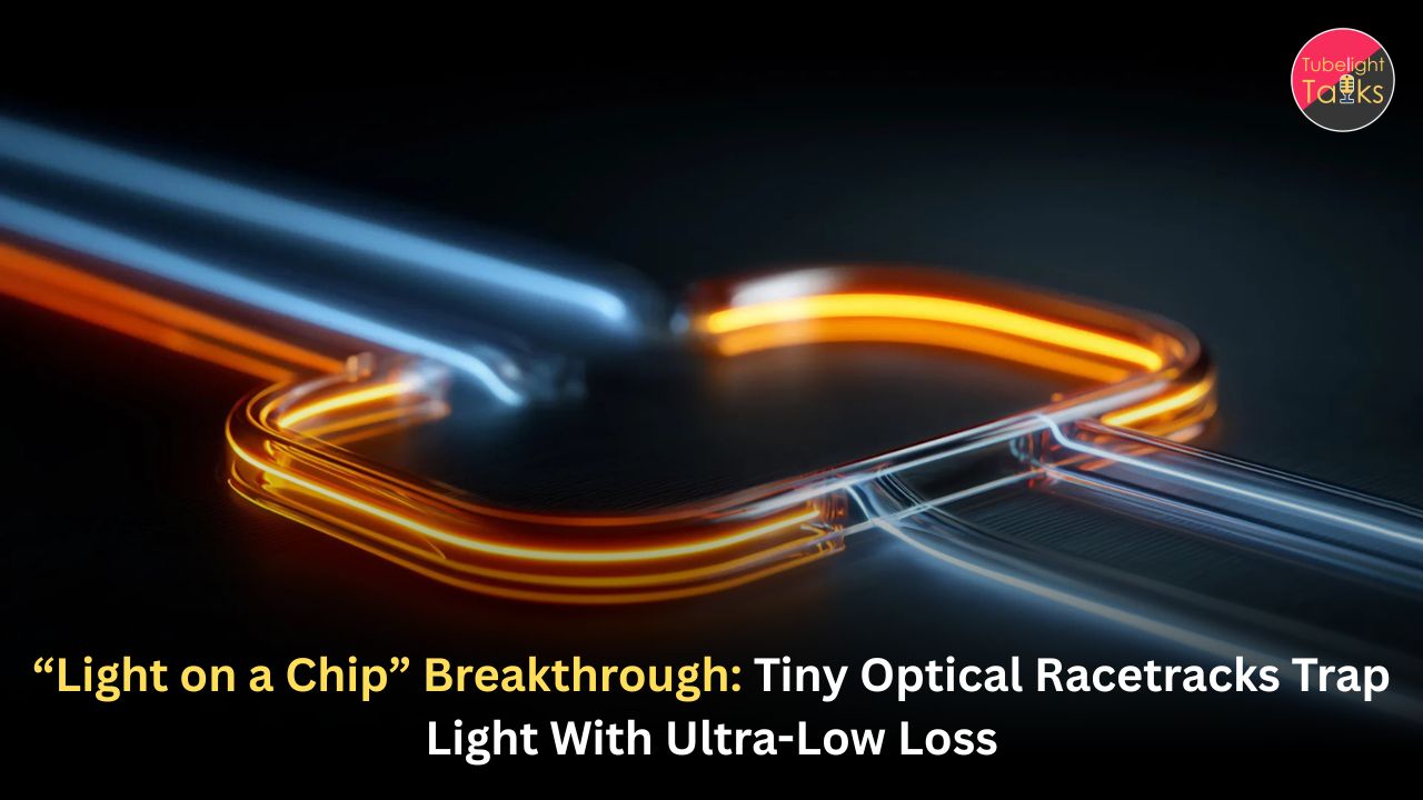
An optical racetrack microresonator is a tiny loop-shaped structure – often just microns wide – etched or deposited on a chip. Light enters the loop and, if the resonator is well-designed, keeps circulating like a runner doing laps. Each lap builds intensity inside the device, enabling powerful optical effects even with modest input power.
CU Boulder describes the microresonator concept plainly: it traps light and “build[s] up its intensity,” which allows “unique light operations” once the intensity gets high enough.
Why microresonators are “small devices with big consequences”
Microresonators are foundational components in modern photonics. When you can keep light circulating longer, you can do more with it:
- detect tiny chemical signatures for sensing,
- create compact microlasers,
- shape light into precise frequencies,
- support ultra-stable timing and measurement systems,
- strengthen photonic links that move data efficiently.
That’s why “light on a chip” breakthroughs matter: they push the digital world toward faster, lower-power optical systems – especially as computing and AI workloads keep expanding.
The Real Enemy: Loss
“Loss” is how photonic dreams get diluted
In any optical circuit, “loss” is the part of the light signal that disappears – absorbed as heat, scattered by rough surfaces, or leaked away at bends and junctions. On a chip, even tiny imperfections can cause big problems because the structures are extremely small. CU Boulder notes that many photonic devices are smaller than the width of a sheet of paper, and even dust or surface flaws can disrupt how light travels.
Why low loss is the difference between “possible” and “practical”
The CU Boulder team’s goal is explicitly about lowering the power needed to get useful behavior from microresonators. As lead author Bright Lu puts it:
“Our work is about using less optical power with these resonators for future uses.”
That one line explains why this story is trending in “technology for good” circles: lower optical power can mean lower energy cost and more scalable real-world deployment.
The Key Innovation: Euler Curves (Highway Geometry, Photonics Impact)
Light can’t do right-angle turns
The most shareable element of this research is also the most intuitive. The team used “Euler curves” – smooth curves common in roads and railway design – because light behaves badly at abrupt corners. CU Boulder explains it in everyday logic: just as cars can’t make sharp right-angle turns at speed, light can’t be forced into abrupt bends.
How Euler curves reduce bending loss
When light is guided through a waveguide, it behaves like a wave confined within the material. Sharp bends cause the guided mode to mismatch and radiate outward – effectively leaking energy. By using smoothly changing curvature, the resonator reduces that “mode shock,” so photons stay in the track longer.
Won Park, a co-advisor, summarized the payoff clearly:
“These racetrack curves minimize bending loss.”
Why this is a design philosophy shift
This isn’t only a materials story or a manufacturing story. It’s a reminder that performance can come from geometry – careful, physics-aware shaping that respects how waves behave. That makes the breakthrough feel replicable: other labs and companies can apply similar principles to different materials and chip platforms.
Also Read: AI Mental Health Ecosystem: How Technology Is Becoming a Lifeline in 2025
The Material Choice: Why Chalcogenide Glass Matters
A “semiconductor glass” with photonics advantages
A major success highlighted by CU Boulder is the team’s use of chalcogenides – specialized semiconductor glasses known for high optical transparency and strong nonlinear behavior. Won Park describes them as excellent for photonics due to “high transparency and nonlinearity.”
Try Free Universal CPM Calculator for Ad Spend & Revenue
Chalcogenide platforms are especially interesting because they can support nonlinear optics – useful for frequency generation, signal processing, and compact laser systems.
But it’s not easy to work with
The same release emphasizes a practical truth: chalcogenides are “not easy to process,” requiring careful fabrication. Professor Juliet Gopinath describes them as “difficult, but rewarding,” and links the new results directly to bend-loss reduction.
This combination – hard material, smart geometry – helps explain why the achievement stands out.
The Numbers Behind the Excitement
What “ultrahigh-Q” means in plain language
Microresonator quality is often discussed in terms of the “Q factor,” a measure of how long light can stay circulating before it decays. Higher Q generally means lower loss and stronger resonance behavior.
The team’s preprint describes a chalcogenide micro-racetrack resonator using Euler curves with:
- absorption loss of 0.43 dB/m,
- intrinsic quality factor of about 4.5 × 10⁶,
- waveguide cross-section less than 1 μm².
On a chip that’s only centimeters across, talking about “loss per meter” may sound strange – but that’s exactly the point: when light circulates repeatedly in a resonator, its effective travel distance can become extremely long. Lower loss per unit length becomes decisive. (You’ll see this same logic echoed in another major photonics breakthrough from Caltech, discussed below.)
Why “almost zero energy loss” is a fair public takeaway
No real device has literally zero loss. But “ultra-low loss” in chip photonics can feel “almost zero” compared to typical on-chip constraints – especially when the performance reaches the top tier for a given material platform. CU Boulder explicitly frames their resonators as “high-performing” and emphasizes how the geometry “dramatically reduced light loss.”
What Can You Do With Light That Stays Put?
1) Sensors that become smaller, more sensitive, and lower power
Microresonators are powerful sensors because tiny changes – temperature, chemicals, motion – can shift resonance properties. When resonances become “deep and narrow,” it’s easier to detect small shifts.
A CU Boulder researcher describes the “needle-like” resonance shape they were chasing, and how seeing sharp resonances made them realize they had “finally cracked the code.”
Bright Lu also points to future sensor uses “from navigation to identifying chemicals.”
2) Microlasers and tunable photonic systems
CU Boulder notes potential for compact microlasers and photonic systems that can be tuned and integrated more easily.
High-Q resonators can support narrow-linewidth laser behavior and nonlinear effects that help generate or stabilize light – important for precision measurement and communications.
3) Photonic building blocks that “tie the pieces together”
A key point in the CU Boulder release is integration: microresonators help connect lasers, modulators, and detectors into systems manufacturers can scale. Lu notes the longer-term goal is to build something that can be handed to a manufacturer to create “hundreds of thousands” of devices.
That scaling angle is part of why this is trending: it’s not just a lab curiosity – it’s being framed as manufacturable photonics.
Why This Matters for Greener, Faster Digital Infrastructure
Today’s bottleneck: energy and heat
Even without quoting global statistics, the challenge is widely understood: modern computing systems burn significant energy and produce heat, and data movement (not just computation) is a major contributor to inefficiency. Photonics is attractive because light can carry vast data with low resistance and minimal heating – especially over distance.
When chip photonics becomes low-loss and efficient, it strengthens the case for shifting more data handling and signal processing into optical domains, reducing reliance on power-hungry conversions and amplifications.
The photonics trendline is clear
This CU Boulder breakthrough sits inside a broader wave of “ultra-low-loss photonics” advances. A standout example is Caltech’s February 2026 announcement of guiding light on silicon wafers with loss “approaching that of optical fiber” at visible wavelengths, enabled by printing fiber-like glass circuits onto wafers and reflowing surfaces for extreme smoothness.
Caltech explicitly ties such low-loss photonic integrated circuits to applications including “AI data-center communications” and “quantum computing.”
Why both stories point to the same future
CU Boulder’s racetrack resonators show how geometry and fabrication precision can slash bend losses in a challenging nonlinear material platform. Caltech shows how fiber-like glass materials and wafer processes can push losses toward the “negligible” regime across wide visible-to-near-IR bands.
Together, the message is powerful:
If photonic chips can approach fiber-like efficiency while staying manufacturable, the energy cost of moving information can drop – without sacrificing speed or precision.
How They Built It: Precision Fabrication as a Core Ingredient
Why electron-beam lithography shows up in the story
CU Boulder’s team used a new electron-beam lithography system in a cleanroom facility (COSINC). They emphasize that traditional lithography is limited by light’s wavelength, while electron-beam lithography enables sub-nanometer resolution – critical when small surface imperfections can create scattering loss.
This manufacturing detail matters for the “technology for good” angle: scalable energy-efficient photonics depends on reliable fabrication, not one-off hero devices.
Measurement and validation: looking for the “dips”
After fabrication, the team tested the microresonators using laser-based measurements, looking for resonance signatures – “dips” in transmitted light – then analyzing their shape to extract absorption and thermal effects.
This is important because it shows the work isn’t only theoretical; it’s experimentally characterized with metrics tied to real device behavior.
What Still Needs to Happen Before Your Devices Feel This Breakthrough
Integration with broader chip ecosystems
Even great resonators must connect to other components: lasers, modulators, detectors, and packaging that can survive real-world environments. CU Boulder itself describes microresonators as components that help “tie all of those pieces together,” with an eye toward manufacturability.
Robustness and mass production
Chalcogenide materials can be rewarding but challenging to process consistently. Scaling from cleanroom prototypes to high-volume manufacturing will require:
- process repeatability,
- stable material deposition and etching,
- consistent coupling to external fibers or lasers,
- packaging that keeps performance intact over time.
The fact that the research team is already talking in manufacturing language is encouraging – but it’s also a reminder that photonics is as much an engineering discipline as a physics discipline.
Avoiding hype: what this does
not automatically guarantee
It’s tempting to jump from “ultra-low loss” to “100× faster internet.” In reality, speed improvements depend on full-system design: modulation formats, network routing, electronics, protocols, and end-user infrastructure.
What this breakthrough truly strengthens is the foundation: lower-loss photonic building blocks make future high-bandwidth, lower-power systems more feasible.
Why This is Relevant Now
1) The metaphor is irresistible – and accurate
“Highway curves for light” is a rare science story that the public immediately understands. It’s also true: smoother paths reduce loss.
2) It fits the moment: efficiency is the new performance
The tech world is increasingly obsessed with not just “more power,” but “less waste.” The CU Boulder team’s focus on using less optical power speaks directly to that mood.
3) It feels like a hopeful blueprint
Unlike many grand tech promises, this one is built on tangible ingredients:
- a clear design change (Euler curves),
- a clear measurement outcome (ultra-low loss / high-Q),
- clear applications (sensors, microlasers, quantum tools).
Guiding Power Without Waste
A striking lesson from this “light on a chip” breakthrough is that real progress often comes from discipline and precision – not brute force. Instead of pushing more energy into a system and accepting waste, the researchers refined the path so energy stays useful.
In the teachings shared by Sant Rampal Ji Maharaj, there is a strong emphasis on self-control, responsible living, and reducing wasteful habits – because uncontrolled “loss” in life (anger, greed, distraction) quietly drains a person’s potential just as scattering loss drains a signal.
When direction becomes smooth, purposeful, and ethical, power stops leaking into harm and starts creating benefit. In that way, this photonics advance mirrors a deeper truth: the best strength is the one that is guided wisely.
FAQs: Optical Racetrack Microresonator
What is an optical racetrack microresonator?
It’s a tiny loop-shaped on-chip structure that traps light so it circulates repeatedly, building intensity and enabling advanced photonic functions.
What was the key design improvement in this breakthrough?
Using smooth “Euler curves” (like road/railway curves) to reduce bending loss so light leaks out far less at turns.
What performance did the team report?
Their preprint reports ~0.43 dB/m absorption loss and an intrinsic Q around 4.5 × 10⁶ in a very small waveguide cross-section.
What could this enable in real life?
Lower-power, more sensitive sensors; compact microlasers; and stronger building blocks for photonic integrated circuits used in communications and advanced measurement.
Is this part of a wider trend in ultra-low-loss photonic chips?
Yes – recent work from Caltech also reports fiber-like low-loss photonic circuits on silicon wafers, aimed at applications including AI data-center communications and precision measurement.
Related Stories


Discussion (0)