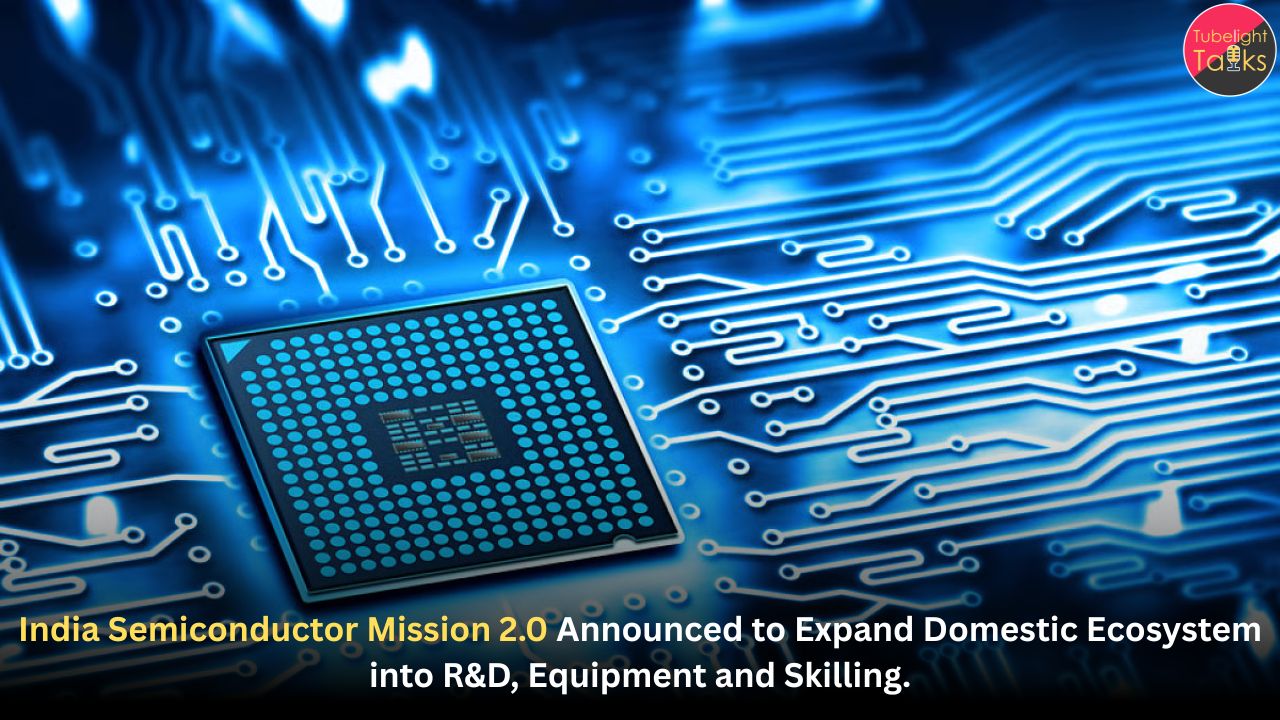
Technological Growth: India Semiconductor Mission 2.0 Broadens the Chip Strategy
The government has announced India Semiconductor Mission 2.0 as a major next step in the country’s effort to build a deeper semiconductor ecosystem. PIB’s official note says the new phase will focus on semiconductor equipment and materials, full-stack Indian semiconductor intellectual property, stronger supply chains, and industry-led research and training centres to create a future-ready skilled workforce. A provision of ₹1,000 crore has been made for ISM 2.0 in FY 2026–27.
Mission 2.0 is broader than the first phase
PIB says ISM 1.0 helped expand India’s design capabilities and advance fabrication, assembly and testing infrastructure. ISM 2.0 is now designed to deepen those gains by moving into more strategic layers of the ecosystem. That includes not only production support, but also equipment, materials and domestic design capability.
This matters because semiconductor strength does not come only from building fabs. It comes from how much of the value chain a country can control or supply. Mission 2.0 clearly aims to move India further up that chain. This is an inference, but it follows directly from the official focus areas laid out by PIB.
R&D and skilling are central, not peripheral
The official PIB note says the ₹1,000 crore provision comes with strong emphasis on industry-led research and training centres to drive technology development and create a future-ready skilled workforce. That means Mission 2.0 is not only industrial policy. It is also a capability-building policy.
This is especially important because semiconductor ecosystems fail when they rely only on capital expenditure without building engineers, researchers and process talent. The government’s inclusion of research and training centres suggests it understands that domestic semiconductor ambition needs people, not just plants.
Also Read: Global AI Chip Realignment: Major Tech Company Launches New Semiconductor Plant Overseas
Equipment and materials are a strategic shift
One of the strongest new features in the official description is the focus on producing semiconductor equipment and materials in India. That is a meaningful change because these segments are often harder to localise than assembly operations and tend to be dominated by a small number of countries and firms globally.
If India can build serious presence in these layers, it would improve supply resilience and reduce dependence on external bottlenecks. That will not happen quickly, but Mission 2.0 clearly signals that the government wants to attempt exactly that. This is an inference, but it is strongly grounded in the PIB description.
Full-stack design IP is a long-term play
PIB also says ISM 2.0 will focus on designing full-stack Indian semiconductor intellectual property. That is one of the most strategically ambitious parts of the mission. Design IP shapes how much value a country captures even when physical manufacturing is shared across global partners.
That means the mission is trying to ensure India is not only a location for semiconductor operations, but also a source of original capability. Over time, that may matter as much as fabrication itself.
Why this matters for India’s tech future
Semiconductors sit under electronics, telecom, defence, automobiles and AI systems. PIB explicitly says chips underpin every critical digital and industrial system. So this mission is not a niche policy. It is foundational infrastructure for the wider economy.
The significance of Mission 2.0 lies in its attempt to shift India from participation to depth. The success of that shift will depend on execution, but the policy direction is now unmistakable.
Real growth is built through patient capability
Technology leadership is rarely created by one announcement. It grows through training, research, discipline and long-term commitment. Mission 2.0 reflects that reality: durable strength comes when knowledge, production and human skill grow together.
Call to Action
The next step to watch is implementation. The real test of ISM 2.0 will be whether India can quickly convert the policy vision into working research centres, supplier capacity, talent pipelines and production partnerships that endure beyond announcements.
FAQs: India Semiconductor Mission 2.0
1. What is India Semiconductor Mission 2.0?
It is the new phase of India’s semiconductor strategy announced in the Union Budget 2026–27 framework and described in official PIB material.
2. What are its main focus areas?
Equipment and materials, full-stack design IP, supply chains, and industry-led research and training centres.
3. How much money has been provided for FY 2026–27?
₹1,000 crore, according to PIB.
4. Does the mission include skilling?
Yes. PIB says it strongly emphasizes research and training centres to create a future-ready skilled workforce.
5. Is this only about fabrication plants?
No. The official plan is broader and includes materials, equipment, design IP and R&D.
6. Why is this important?
Because semiconductors underpin critical digital and industrial systems across the economy.
Related Stories


Discussion (0)