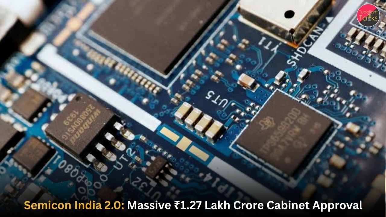
Union Cabinet Approves Semicon India 2.0 with ₹1.27 Lakh Crore Outlay
The Union Cabinet, chaired by Prime Minister Narendra Modi, has officially approved Semicon India 2.0 with a total financial outlay of ₹1,27,500 crore. This landmark decision reinforces India’s commitment to building an end-to-end semiconductor ecosystem, positioning the nation as a globally trusted hub for chip design, fabrication, and packaging.
Building on the momentum generated under the initial phase of the India Semiconductor Mission (ISM), Semicon India 2.0 shifts focus from establishing basic infrastructure to creating a self-sustaining supply chain. The initiative aims to reduce strategic import dependencies in critical sectors such as artificial intelligence (AI), 5G/6G communications, automotive, and defense systems.
Also Read: The Rise of Digital India: How Technology Is Empowering Every Citizen
The 6 Strategic Pillars of the Semicon India 2.0 Programme
To ensure a comprehensive ecosystem approach, the Ministry of Electronics and Information Technology (MeitY) has structured the second phase around six core pillars:
- Chip Design & Intellectual Property (IP): Expanding support for startups and MSMEs to develop indigenous chip designs, compute architectures, and commercial intellectual property.
- Manufacturing Equipment & Materials: Incentivizing domestic manufacturing of raw materials, specialty chemicals, industrial gases, and precision machinery required for semiconductor fabrication.
- Semiconductor Fabrication Capacity: Accelerating the setup of commercial silicon fabs, compound semiconductor facilities, and discrete component units.
- Advanced Packaging (ATMP/OSAT): Strengthening Assembly, Testing, Marking, and Packaging (ATMP) units to make India an international alternative for chip packaging.
- Research & Development: Focusing on sub-28nm advanced nodes, silicon photonics, and next-generation chiplet architectures in partnership with premier global research institutions.
- Talent Development: Scaling specialized engineering skill sets across Indian universities to build a workforce ready for high-tech semiconductor manufacturing.
Comparing India Semiconductor Mission 1.0 vs. Semicon India 2.0
The transition from ISM 1.0 to Semicon India 2.0 reflects India’s evolving technological maturity, moving from foundational incentives to holistic supply chain independence.
| Parameter | Semicon India 1.0 (Phase 1) | Semicon India 2.0 (Phase 2) |
| Budgetary Outlay | ₹76,000 Crore | ₹1,27,500 Crore |
| Primary Scope | Initial Fab Setup & OSAT Units | Full Supply Chain (Equipment, Chemicals, IP, Fabs) |
| Target Investment | ~₹1.64 Lakh Crore Catalyzed | ₹4.00 Lakh Crore Expected |
| Focus Node Range | 28nm – 110nm Legacy Nodes | Advanced Nodes, Chiplets & Specialized Fabs |
| Design Incentive Support | Financial aid for select startups | IP creation, EDA tool access, and Tape-out incentives |
Economic Impact, Global Supply Chains, and Job Creation
Government estimates indicate that the ₹1.27 lakh crore policy push under Semicon India 2.0 will catalyze total investments exceeding ₹4 lakh crore and generate direct semiconductor output worth ₹2 lakh crore.
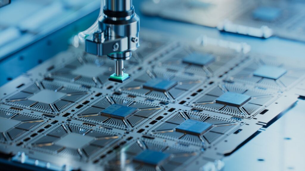
This expansion comes at a pivotal juncture as global electronics manufacturers seek resilient supply chains. By building local capacity for raw materials, specialty gases, and advanced assembly, India mitigates global chip shortages while generating thousands of high-skilled engineering jobs.
For further details on government policy notifications, visit the official India Semiconductor Mission Portal.
Also Read: BRICS Expansion 2026 The Expanded 11-Nation Bloc Reshapes Global Economic Order
Beyond Technological Supremacy: Navigating Human Fulfillment in an Automated World
While technological breakthroughs like Semicon India 2.0 showcase humanity’s remarkable intellectual capability to build faster microprocessors and smart machines, material advancement alone cannot resolve the core challenges of human existence. Despite rising economic wealth and technological convenience, society faces unprecedented levels of mental stress, anxiety, global instability, and existential uncertainty.
Humanity often falls into the trap of seeking ultimate happiness through material progress and worldly achievements. True stability and lasting peace cannot be manufactured in cleanrooms or engineered through silicon chips. According to the sacred spiritual discourses of Sant Rampal Ji Maharaj, material developments are temporary remedies for physical life, whereas genuine liberation from suffering requires spiritual enlightenment and connection with Supreme God Kabir.
Sant Rampal Ji Maharaj emphasizes that worshipping according to authentic scriptures brings internal peace, moral clarity, and protection from life’s inevitable anxieties. While nations strive for economic self-reliance, individuals must seek spiritual self-realization to achieve permanent joy and freedom from the endless cycle of birth and death.
To explore deeper spiritual knowledge and discover the path to lasting peace, watch the official discourses on the Official YouTube Channel of Sant Rampal Ji Maharaj.
Frequently Asked Questions (FAQs) on Semicon India 2.0
Q. What is the total budget outlay approved for Semicon India 2.0?
The Union Cabinet has approved Semicon India 2.0 with a total financial outlay of ₹1,27,500 crore (₹1.27 lakh crore).
Q. What are the main objectives of the Semicon India 2.0 scheme?
The scheme aims to strengthen India’s end-to-end semiconductor ecosystem by supporting domestic chip design, manufacturing equipment, raw materials, semiconductor fabrication, and advanced packaging.
Q. How does Semicon 2.0 differ from the first phase of the India Semiconductor Mission?
While Phase 1 focused primarily on attracting initial fab projects and OSAT facilities, Semicon 2.0 expands coverage to critical equipment, specialty chemicals, IP creation, and advanced node research.
Q. How much private investment is expected to be catalyzed by this scheme?
The government expects the ₹1.27 lakh crore public outlay to attract total sector investments worth approximately ₹4 lakh crore, yielding semiconductor output worth ₹2 lakh crore.
Q. Which key industries will benefit most from domestic semiconductor production?
Key sectors include artificial intelligence (AI), 5G/6G telecommunications, electric vehicles (EVs), defense systems, medical devices, and
Related Stories










Discussion (0)