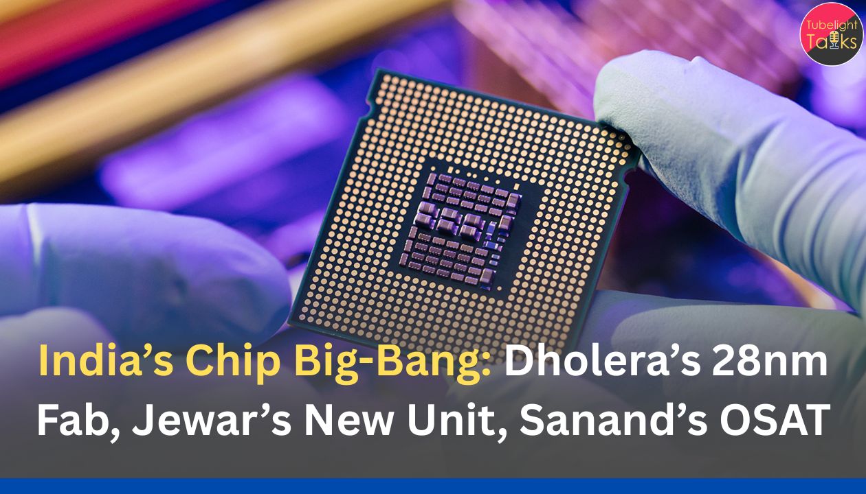
India’s Chip Big-Bang: Dholera’s 28nm Fab, Jewar’s New Unit, Sanand’s OSAT—and the 2025 Playbook with Official Sources
India’s Chip Big-Bang: India’s semiconductor story accelerated in 2024–25 from intent to implement. The Union Cabinet cleared three units in February 2024—including Tata–PSMC’s 28nm fab at Dholera and two ATMP/OSAT facilities—and later approved a sixth unit in May 2025: HCL–Foxconn near Jewar. In parallel, Micron’s OSAT campus at Sanand advanced, and CG Power–Renesas launched a pilot line in Gujarat—evidence that packaging and testing are materialising ahead of large-scale wafer output.
This explainer stitches together what’s official, where construction stands, capacities, jobs, and timelines—using only PIB/ISM and primary partner releases—so newsrooms and analysts can cite, compare, and forecast with confidence.
The Official Ledger: What’s Been Approved and Announced
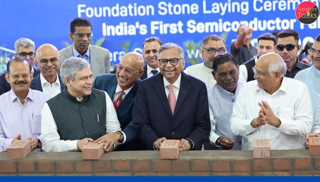
1) Tata–PSMC 28nm Fab at Dholera, Gujarat (Logic & Power)
- Status: Approved by the Union Cabinet on Feb 29, 2024 under the Semicon programme.
- Capacity: 50,000 WSPM (wafer starts per month).
- Node / Segments: 28nm logic (high-performance compute) and power management chips for EVs, telecom, defence, automotive, consumer electronics & displays.
- Investment: ₹91,000 crore, with PSMC (Taiwan) as tech partner.
- Why it matters: Places India’s first commercial logic fab on a mature, globally demanded node; 28nm remains a workhorse for autos, industrial, and many consumer designs.
2) Tata Semiconductor Assembly & Test (TSAT) at Morigaon, Assam
- Status: Approved Feb 29, 2024.
- Investment: ₹27,000 crore; indigenous packaging including flip-chip and ISIP targeted.
- Capacity: 48 million units/day (packaging). Use-cases span automotive, EVs, consumer, telecom, mobiles.
3) CG Power–Renesas–Stars Microelectronics OSAT at Sanand, Gujarat
- Status: Approved Feb 29, 2024; 2025 saw pilot line launch at Sanand.
- Investment: ₹7,600 crore; Renesas brings microcontroller/analog/power SoC pedigree.
- Capacity: 15 million units/day (packaging). Segments: consumer, industrial, auto, power.
4) HCL–Foxconn at Jewar (YEIDA), Uttar Pradesh
Sixth unit
- Status: Approved May 14, 2025; plant near Noida International (Jewar) Airport.
- Product: Display driver ICs (DDIs) for phones, laptops, autos, PCs & other screens.
- Capacity: 20,000 wafers/month, 36 million chips/month design output.
- Investment: ₹3,700 crore per PIB (other reports cite ~₹3,706 crore).
- Additional coverage: Reuters called it India’s sixth approved unit; production target 2027; complements Tata/Micron moves.
5) Micron OSAT at Sanand, Gujarat – Construction & Jobs
- Official anchor: Project announced June 2023; Govt/PIB updated in Dec 2023 on construction pace and job numbers.
- What Micron said: The assembly/test facility will package DRAM & NAND products for domestic and global markets.
- Govt signal: Up to 5,000 direct and 15,000 indirect jobs; training pipeline for ~10,000 engineers in Gujarat aligned to the project.
6) India Semiconductor Mission (ISM) & SEMICON India 2025
The ₹76,000-crore programme under ISM is the umbrella for fab/OSAT incentives; the 2025 industry platform (SEMICON India) showcased partner momentum (ISM, SEMI, global suppliers). Use ISM pages for official references.
Timelines, Milestones & Realistic Expectations (2025–2027)
Dholera (Tata–PSMC 28nm)
- 2024 approval → construction → equipment install/qualification → ramp. Mature-node fabs often take ~2–3 years from groundbreaking to first commercial wafers, then another year to stable yields. Watch for tool move-in and pilot lots updates via official channels.
Jewar (HCL–Foxconn DDIs)
- Approval May 2025; Reuters noted a 2027 production start; PIB lists capacity/throughput specifics. Expect construction, cleanroom build, tool install through 2026–27.
Sanand (Micron OSAT; CG Power–Renesas)
- Micron: construction advanced through 2024–25; multiple reports pointed to first packaged chips “in 2025/early 2026”; rely on Micron/PIB updates for confirmation.
- CG Power–Renesas: pilot line launched (Aug 2025)—a stepping stone toward volume OSAT.
Who Needs These Chips (and Why 28nm Still Matters)
- Automotive & EVs: Power management ICs, microcontrollers, and safety components are not on bleeding-edge nodes. 28nm and larger processes dominate for reliability & cost. This is Dholera’s sweet spot.
- Telecom & Power Electronics: PMICs and analog mixed-signal chips (e.g., for 5G infra, chargers, UPS, industrial drives) map to 28–90nm and specialty processes; OSAT is critical for advanced packages.
- Consumer/PC/Displays: HCL–Foxconn’s display-driver ICs tie directly into TV/monitor/phone supply chains—an import-substitution and export story in one.
Jobs, Skill Pipelines & Ecosystem Suppliers
- PIB tallies for the three Feb 2024 units project ~20,000 direct and ~60,000 indirect jobs, with spillovers into auto, telecom, industrial & consumer electronics.
- Micron Sanand: Govt note cites 5,000 direct + 15,000 indirect jobs and training for ~10,000 engineers.
- Equipment & gases: PIB’s Jewar release name-checks Applied Materials, Lam Research, Merck, Linde, Air Liquide, Inox, etc., as ecosystem players ramping India presence.
- Centres of excellence: Applied Materials signalled expanded India engineering/R&D footprints supporting tool development and talent pipelines.
How to Read Capacity Numbers without Tripping
WSPM vs Units/Day
- Fab: capacity is in WSPM. A 50k WSPM fab doesn’t translate linearly to chips/year; yield, product mix and die size matter. (Dholera: 50k WSPM).
- OSAT: capacities appear as units/day—they reflect package output; different packages (QFN/BGA/FCBGA) have very different cycle times. (Assam: 48M/day, CG Power: 15M/day).
Pilot Line ≠ Full Ramp
A pilot line proves processes and trains staff; it’s the bridge to volume OSAT. Sanand’s pilot launch signals process maturity, not full capacity.
The Policy Chassis: ISM, Incentives, and the 76k-Crore Programme
The India Semiconductor Mission coordinates fiscal support, program governance and partner engagement under the ₹76,000-crore Semicon scheme. For newsroom accuracy, cite ISM’s pages for programme framing and SEMICON India briefings for stakeholder lists/announcements.
State Map (2025): Who’s Doing What
- Gujarat: Dholera 28nm fab (Tata–PSMC); Sanand hosts Micron OSAT and CG Power–Renesas.
- Assam: TSAT OSAT at Morigaon.
- Uttar Pradesh: HCL–Foxconn near Jewar.
- Karnataka: Supplier/R&D ecosystems expanding (equipment and design). (Use state/press items carefully; for official framing, lean on ISM + company releases).
Risks & Reality Checks
- Schedule risk: Fabs have long lead times for tools/utilities; commissioning slips are common worldwide. Anchor to official milestones, not speculative timelines.
- Talent gap: Government repeatedly flags a global fab/OSAT skills shortfall—India is positioning to bridge it, but training pipelines take time.
- Demand cycles: Semis are cyclical. Mature nodes for autos/industrial are resilient, but swings happen; OSAT utilisation will vary by package mix.
- Supply chain depth: Chemicals, specialty gases, CMP slurries, photomasks and spares ecosystems must localise over time; PIB hints at suppliers stepping in.
Practical Playbook for Companies in India (2025–27)
If you’re an OEM (auto, consumer, telecom)
- Map bill-of-materials to 28–90nm and power/analog; identify packages likely to be supported by Assam/Sanand OSAT lines.
- Qualify second sources early; fab/OSAT ramps need reliability qual (AEC-Q100 for autos, JEDEC).
- Co-develop package variants to suit Indian thermal/EMI conditions; loop in OSATs for DFX (design for assembly/test).
If you’re a design house (fabless)
- Tape-out roadmaps to nodes available in India’s pipeline (28nm and above), align with power/analog IP; prepare test vectors and ATE plans for Indian OSATs.
- Engage ISM programmes and university labs for talent; plug into vendor initiatives (e.g., toolmaker collaborations).
If you’re a state/cluster developer
- Utilties first (power quality, water, UPW, waste): OSATs tolerate less extreme utilities than fabs but still need stable lines and industrial gases.
- Build supplier parks for leadframes, substrates, molding compounds, trays—the small stuff that keeps OSATs ticking.
Frequently misunderstood (and easy fixes)
- “28nm is outdated.” Not for autos/power/industrial—28nm is a durable sweet spot with long lifecycles and stringent reliability needs. Dholera is aimed precisely here.
- “OSAT means low value.” Packaging/testing determine reliability and thermal performance—mission-critical for automotive and power devices; it’s where India is ramping fastest.
- “Sixth unit = six fabs.” The mix includes one logic fab + multiple OSAT units. Read each PIB note’s product/capacity carefully.
Building High-Tech with High Values
Manufacturing semiconductors is precision engineering—but the foundations are human conduct: honesty in procurement, on-time wages, safety discipline, and respect up and down the line. Values-first guidance that emphasises truthful work, non-exploitation, and responsibility helps factories and teams make the right call when nobody’s watching—whether that is reporting a near-miss, refusing to shortcut ESD/cleanroom norms, or crediting a supplier fairly.
For readers who want that lens, explore the enlightened Sant Rampal Ji Maharaj book “Way of Living” and discourses on ideal behaviour for employers and employees, which centre simple, practical conduct that keeps complex systems trustworthy.
Read Also: Global AI Chip Realignment: Major Tech Company Launches New Semiconductor Plant Overseas
FAQs: Semiconductor Units In India
Q1. How many semiconductor units has India officially approved as of 2025?
Six. Three on Feb 29, 2024 (Tata–PSMC Dholera fab; TSAT Assam OSAT; CG Power–Renesas OSAT) and another on May 14, 2025 (HCL–Foxconn at Jewar); the rest stem from earlier approvals (e.g., Micron Sanand).
Q2. What exactly will the Dholera fab make?
A 28nm logic fab with power-management chips across EV/auto, telecom, defence, and consumer electronics—50,000 WSPM capacity in the plan.
Q3. Are we making chips or only packaging?
Both. India is standing up OSAT first (Micron, CG Power–Renesas, TSAT) while the Dholera fab constructs—the standard path for new ecosystems.
Q4. What’s special about the HCL–Foxconn Jewar unit?
It targets display driver ICs—vital for screens in phones/TVs/autos—with 20k wafers/month and 36M chips/month design output.
Q5. How many jobs could this create?
PIB estimates: ~20k direct + 60k indirect for the Feb-2024 approvals; Micron Sanand adds 5k direct + 15k indirect. Actuals depend on ramps and suppliers.
Q6. Where do I find authentic programme details?
Use PIB releases for approvals and ISM for programme framing; rely on company press rooms for project-specific statements.
Q7. When will India ship its first logic wafers domestically?
Dholera is the first large logic fab; exact “first wafer” depends on construction, tool install and qual. Track Tata–PSMC/PIB updates; avoid guessing dates.
Q8. What should firms do now to benefit?
Lock DFX with Indian OSATs, line up reliability quals, plan dual-source contracts, and join ISM/SEMI platforms to access supplier networks.
Related Stories


Discussion (0)