Ultrathin Transistor Material: The Research & Its Significance
Ultrathin Transistor Material: The research team at the University of Chicago, in collaboration with Argonne National Laboratory, fabricated a transistor device that uses a layer of atomically thin semiconductor topped by a sheet of molecular crystal. Unlike traditional transistors which rely on stacking diverse semiconductor materials (n‑type/ p‑type), this device leverages charge localization—a phenomenon where electrons become confined in a region—at room temperature. Previously, this effect required cryogenic conditions.
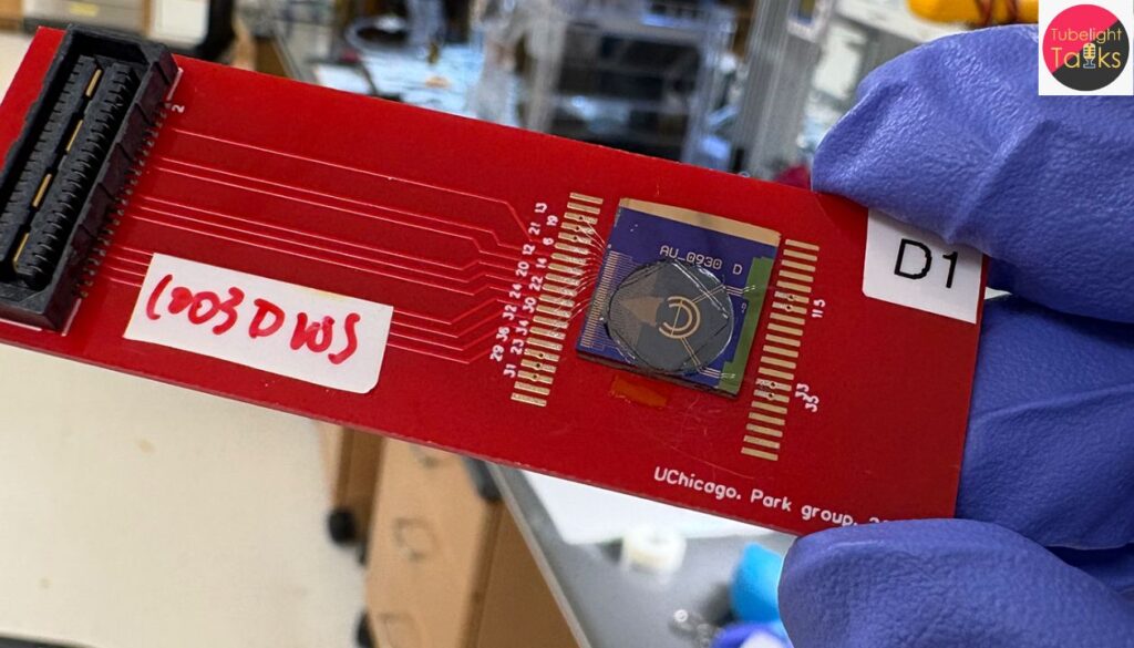
The entire active portion of the device is only four atoms thick. Remarkably, its performance was measured to be comparable to high‑quality traditional transistors.
Technical Highlights
- Room‑temperature operation: no need for ultra‑low temperatures.
- Simplified architecture: fewer layers, less complexity.
- Potential for lower voltage, lower power consumption: early tests show promising efficiency.
- Compactness: atomic‑scale thickness opens door to ultra‑miniaturised electronics, flexible or wearable devices.
Why This Breakthrough Matters
Electronics Scaling and Moore’s Law
As semiconductor technology pushes into deeper nanometre scales, physical limits and heat‑dissipation issues become more pressing. A transistor only a few atoms thick addresses some of those constraints directly.
Power Efficiency & Device Form‑Factors
Thin devices consume less power and can be integrated into flexible substrates, wearable electronics, even biological sensors. Reduced power means less heat and greater reliability.
New Device Paradigms
With simplified architecture and novel mechanism (charge localization rather than standard doping), this opens avenues for alternative computing paradigms (perhaps quantum, neuromorphic or novel logic devices).
Strategic Technological Advantage
For countries and companies investing in advanced materials and devices, early leadership in such ultrathin transistor technologies may translate into competitive edge in consumer electronics, defence, medical devices and more.
Challenges and Next Steps for Ultrathin Transistor Material
Manufacturing and Yield
Lab‑scale success is one thing; mass manufacture of four‑atom‑thick devices is another. Ensuring uniformity, defect‑control and yield at scale will be a challenge.
Integration with Existing Technologies
How will these novel materials interface with current semiconductor ecosystems (interconnects, chip packaging, circuit design)? Transitioning from novelty to viable product may require infrastructure updates.
Reliability & Longevity
Thin materials can be more susceptible to environmental damage (oxygen, moisture), mechanical stress or thermal cycling. Ensuring stability over years of service will be essential.
Cost and Industry Adoption
Even if technically viable, cost‑effectiveness and industry willingness to adopt new materials will determine commercial success. Partnerships between academia and industry will be key.
Align Progress with Responsibility and Purpose
In an era where patents, clusters and high‑tech exports dominate headlines, the teachings of Sant Rampal Ji Maharaj offer an important reminder: true innovation is not just about breakthroughs in technology, but about upliftment of human life, ethical application and shared welfare. When nations race up the innovation ladder, aligning progress with responsibility and purpose becomes essential.
Also Read: Global AI Chip Realignment: Major Tech Company Launches New Semiconductor Plant Overseas
What to Monitor Going Forward
Commercialisation Roadmap
Watch for announcements of prototypes in consumer electronics, wearable devices or specialised sensors using this ultrathin material.
Partnerships & Industry Transfers
Which semiconductor firms, electronics manufacturers or start‑ups partner or license this technology? Collaboration will signal transition from lab to market.
Broader Material Landscape
Will this research spur competing approaches in other institutions (e.g., alternative two‑dimensional materials, organic‑semiconductor hybrids)? Will we see an ecosystem emerge around ultrathin devices?
Global Patent & IP Landscape
New materials often trigger patent‑races. Watch for filings, licensing agreements and standards development.
FAQs: UChicago Ultrathin Transistor Breakthrough
Q1. What is the key innovation of this research?
The development of a transistor device only four atoms thick, combining an atomically thin semiconductor with a molecular crystal sheet, operating at room temperature using charge‑localization.
Q2. Why is the “four‑atoms‑thick” claim significant?
Because it represents an ultra‑miniaturised active device layer that pushes the limits of semiconductor scaling and opens possibilities for new form‑factors and low‑power devices.
Q3. What mechanism does this device use instead of standard doping layers?
It uses charge localization rather than traditional n‑type/p‑type semiconductor layering—this simplifies architecture and offers potential performance gains.
Q4. What sectors could benefit from this development?
Consumer electronics (phones, wearables), medical devices, sensors, flexible electronics, high‑performance computing and possibly quantum/neuromorphic systems.
Q5. What are the major hurdles before commercial use?
Scaling from lab‑prototype to mass production, manufacturing yield, integration with existing semiconductor workflows, cost‑effectiveness and device reliability over time.
Related Stories


Discussion (0)